
Cost-effective ways to reach high-precision flatness after coating
For the fabrication of precision optical plane substrates, when the pitch-lap CMP process on an annular (continuous) polishing machine is used, a diameter-to-thickness ratio D/t ≤ 10:1 (D being the diameter for circular elements and the diagonal length for rectangular elements) allows the surface figure to stably reach PV < 1/10λ. With a properly tuned annular polishing process—and without resorting to magnetorheological finishing (MRF) or ion beam figuring (IBF)—a diameter-to-thickness ratio D/t ≤ 6:1 enables the surface figure to stably reach PV < 1/20λ. After coating, however, the surface figure often degrades to beyond 0.2λ or even worse.
For example, a Φ25 mm fused silica sample with D/t = 10:1 was coated on one side with a multi-cavity bandpass filter coating (high stress); the final post-coating PV exceeded 0.3λ.
The change in surface figure after coating can be roughly estimated using a transformed form of the Stoney equation:
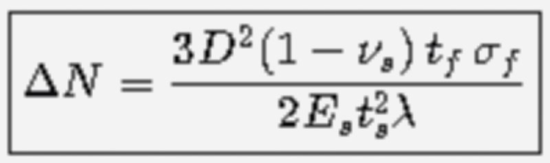
The symbols in the equation are defined as follows:
– ΔN – change in fringe (Newton ring) number caused by coating stress (curvature/defocus term only, per Stoney theory);
– D – effective clear aperture of the optical element;
– nu_s – Poisson's ratio of the substrate;
– t_f – total physical thickness of the film (the sum of the individual layer thicknesses for multilayer coatings);
– sigma_f – biaxial intrinsic film stress (tensile stress positive, compressive stress negative); for multilayer coatings, the equivalent stress is expressed as the sum of the layer thickness–stress products Σ(t_f·sigma_f);
– E_s – Young's modulus of the substrate;
– t_s – substrate thickness;
– λ – wavelength of the test interferometer (typically λ = 632.8 nm).
It follows from this equation that, for comparable film stress levels, the post-coating figure change of an optical element is proportional to the square of the diameter-to-thickness ratio (D/t) and to the total film thickness. Therefore, lens designers should give particular consideration to the diameter-to-thickness ratio when designing high-precision lenses.
In practice, the substrate temperature rises during deposition, which causes redistribution of residual stress in the substrate. This redistribution is uncertain, and the stress superposition in multilayer films is nonlinear; consequently, the prediction accuracy of the Stoney equation is limited. Witness samples coated with the same process are usually used for experimental calibration, and the results are fed back into production. To ensure the accuracy of the final product, the witness-sample calibration often cannot be completed in a single run, which significantly increases cost.
In summary, to keep the post-coating surface figure change small, the following measures can be taken:
1. Increase the lens thickness and reduce the diameter-to-thickness ratio during lens design. Generally, a D/t ratio below 6:1 provides good resistance to figure changes induced by coating stress, ambient temperature variation, and mounting stress. This is the most cost-effective measure.
2. Select substrate materials with a small (1–nu_s)/E_s value (i.e., a high Young's modulus E_s and a suitable Poisson's ratio nu_s). In practice, however, the available choices are very limited once cost and optical material properties are taken into account.
3. Optimize the coating design, taking coating stress into account at the design stage:
1) A symmetric film stack effectively cancels coating stress, e.g., a symmetrically designed anti-reflection (AR) coating;
2) Choose coating materials wisely, pairing compressive-stress and tensile-stress materials (e.g., TiO₂ and SiO₂ have complementary stress characteristics) so that the stresses between layers compensate each other;
3) Optimize the deposition process; the key is to establish a four-parameter process window of “temperature–deposition rate–pressure–IAD power” (IAD: ion-assisted deposition) and identify a low-stress operating regime.
4. Compensation techniques: for thick, high-stress coatings such as broadband all-dielectric high-reflector coatings, multi-cavity narrow bandpass filters, and long-wave infrared (LWIR) dielectric coatings, where the measures above cannot reduce the coating stress to an acceptable level, compensation techniques are required. This is also the most costly approach, and includes the following two methods:
(1) Pre-compensation (pre-shaped polish): coat witness samples with the same process, measure the surface figure before and after coating, and determine the figure change ΔN; use the transformed Stoney equation to calculate sigma_f, predict the post-coating figure change of the production parts, and pre-polish a surface figure opposite in direction to the expected coating deformation;
(2) Backside correction: deposit a correction layer on the back surface of the element, using the stress of the correction layer to counteract the deformation caused by the front-surface coating;
In conclusion, figure change caused by coating stress should be planned for as early as the lens design stage: stress should first be controlled at the source by reducing the diameter-to-thickness ratio, selecting suitable substrate materials, and adopting low-stress coating designs and processes. For high-stress, thick film stacks, compensation means such as pre-compensation, backside correction, or post-coating figuring should be combined, so that the post-coating surface figure accuracy can be ensured at a controllable cost.